


Analog Devices Inc. ADRF5141 High-Power Transmit & Receive Switch ICs
Analog Devices Inc. ADRF5141 High-Power Transmit and Receive Switch ICs are 50Ω reflective SPDT switch ICs manufactured in the silicon process. These switch ICs are intended for transmitting and receiving applications with an integrated power limiter on the receive path. The ADRF5141 switch ICs operate within the 6GHz to 12GHz frequency range. These high-power switch ICs consume a low current of 13μA on the positive supply of 3.3V and 360μA on the negative supply of -3.3V. The ADRF5141 switch ICs use Complementary Metal-Oxide Semiconductor (CMOS)-/Low Voltage Transistor to Transistor Logic (LVTTL)-compatible controls. These switch ICs need no additional driver circuitry, making them a viable alternative to Gallium Nitride (GaN) and PIN diode-based switches.
The ADRF5141 switch ICs feature a fast switching time of 50ns and a fast response and recovery time of <10ns. These switch ICs come in a 20-lead, 3.0mm x 3.0mm, Land Grid Array (LGA) package. The ADRF5141 high-power switch ICs are RoHS compliant and operate within the -40°C to 105°C temperature range. Typical applications include electronic warfare, satellite communications, and radar.
Features
- High-power transmit and receive switch with an integrated power limiter on the receive path
- 6GHz to 12GHz frequency range
- Reflective 50Ω design
- Dual-supply, with no low-frequency spurious
- Low insertion loss:
- TX to ANT:
- 0.9dB at 8GHz to 11GHz frequency range
- ANT to RX:
- 1.4dB at 8GHz to 11GHz frequency range
- TX to ANT:
- High isolation:
- 55dB typical for TX to RX when TX selected
- High-power handling (TCASE = 50°C)
- Input at TX:
- Pulsed 40dBm, >100ns pulse width at 15% duty
cycle
- Pulsed 40dBm, >100ns pulse width at 15% duty
- Input at ANT:
- Pulsed 40dBm, >100ns pulse width at 15%
duty cycle
- Pulsed 40dBm, >100ns pulse width at 15%
- Input at TX:
- High linearity:
- 41dBm input P0.1dB at TX arm
- CMOS-/LVTTL-compatible positive control interface
- Pin compatible with the ADRF5144
Specifications
- Absolute maximum ratings:
- -0.3V to 3.6V positive supply voltage (VDD) range
- -3.6V to 0.3V negative supply voltage (VSS) range
- 135°C junction temperature
- 260°C reflow temperature
- 20-lead, 3mm x 3mm LGA package
- 50ns fast switching time
- <10ns fast response and recovery time
- 17dBm RX flat leakage
- -40°C to 105°C operating temperature range
Applications
- X-band communications and radars
- Electronic warfare
- Satellite communications
- GaN and PIN diode replacement
Functional Block Diagram

Application Diagram

Dimensional Diagram (mm)

Schematic Diagram

Related Evaluation Borad
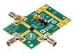
Analog Devices Inc. ADRF5141 Evaluation Board
Designed to evaluate the features and performance of the ADRF514 switch ICs.
Associated Products

Analog Devices Inc. ADRF5142 Silicon SPDT Reflective Switches
Reflective single-pole, double-throw (SPDT) switches manufactured in silicon.
Published: 2022-12-01
| Updated: 2024-07-29