



Infineon Technologies CYT2B9 TRAVEO™ T2G 32-bit Automotive MCUs

Infineon Technologies CYT2B9 TRAVEO™ T2G 32-bit Automotive MCUs are designed for automotive body electronics with processing power and network connectivity built into the Arm® Cortex®-M4F. These MCUs provide higher response and faster communication with the embedded CXPI interface and a CAN FD interface and are ideal for body control modules, HVAC, and lighting. The Infineon TRAVEO devices have advanced security features with the introduction of an HSM (Hardware Security Module), dedicated Cortex®-M0+ for secure processing, and embedded flash in dual bank mode for FOTA requirements. Six power modes enable ECUs to minimize overall power consumption and cutting-edge security features for secure communication with great memory size and pin-count scalability. The MCUs have an optimized software platform for Infineon Autosar MCAL (Microcontroller Abstraction Layer), self-test libraries, Flash EEPROM emulation, and low-level drivers combined with third-party firmware.
Features
- Dual CPU subsystem
- 160MHz (maximum) 32-bit Arm® Cortex®-M4F CPU with
- Single-cycle multiply
- Single-precision floating point unit (FPU)
- Memory protection unit (MPU)
- 100MHz (maximum) 32-bit Arm Cortex M0+ CPU with
- Single-cycle multiply
- Memory protection unit
- Inter-processor communication in hardware
- 3x DMA controllers
- Peripheral DMA controller #0 (P-DMA0) with 92x channels
- Peripheral DMA controller #1 (P-DMA1) with 44x channels
- Memory DMA controller #0 (M-DMA0) with 4x channels
- 160MHz (maximum) 32-bit Arm® Cortex®-M4F CPU with
- Integrated memories
- 2112KB of code-flash with an additional 128KB of work-flash
- Read-While-Write (RWW) allows updating the code-flash/work-flash while executing code from it
- Single- and dual-bank modes (specifically for Firmware update Over The Air [FOTA])
- Flash programming through the SWD/JTAG interface
- 256KB of SRAM with selectable retention granularity
- 2112KB of code-flash with an additional 128KB of work-flash
- Crypto engine (available on select part numbers)
- Supports Enhanced Secure Hardware Extension (eSHE) and Hardware Security Module (HSM)
- Secure boot and authentication
- AES: 128-bit blocks, 128-/192-/256-bit keys
- 3DES: 64-bit blocks, 64-bit key (not available in "eSHE only" parts)
- Vector unit supporting asymmetric key cryptography such as Rivest-Shamir-Adleman (RSA) and Elliptic Curve (ECC) (not available in "eSHE only" parts)
- SHA-1/2/3: SHA-512, SHA-256, and SHA-160 with variable length input data
- CRC: supports CCITT CRC16 and IEEE-802.3 CRC32 (not available in "eSHE only" parts)
- True random number generator (TRNG) and pseudo-random number generator (PRNG)
- Galois/Counter Mode (GCM)
- Functional safety for ASIL-B
- Low-power 2.7V to 5.5V operation
- Wakeup support
- Multiple clock sources
- Communication interfaces
- Up to 8x CAN FD channels
- Up to 8x runtime-reconfigurable SCB (serial communication block) channels, each configurable as I2C, SPI, or UART
- Up to 12x independent LIN channels, LIN protocol compliant with ISO 17987
- Up to 4x CXPI channels with data rates up to 20kbps
- Timers
- Up to 75x 16-bit and 8x 32-bit timer/counter pulse-width modulator (TCPWM) blocks
- Up to 11x Event Generation (EVTGEN) timers supporting cyclic wake-up from DeepSleep, events trigger a specific device operation (such as execution of an interrupt handler, a SAR ADC conversion, and so on)
- Real-time clock (RTC)
- Year/Month/Date, Day-of-week, Hour:Minute:Second fields
- Supports both 12- and 24-hour formats
- Automatic leap-year correction
- I/O
- Up to 152x programmable I/Os
- 2x I/O types
- Regulators
- Generates 1.1V nominal core supply from a 2.7V to 5.5V input supply
- 2x types of regulators
- Programmable analog
- 3x SAR A/D converters with up to 67x external channels (64x I/Os + 3x I/Os for motor control)
- Each ADC supports 12-bit resolution and sampling rates of up to 1Msps
- Each ADC also supports up to 6x internal analog inputs such as:
- Each ADC supports addressing external multiplexers
- Each ADC has a sequencer supporting autonomous scanning of configured channels
- Synchronized sampling of all ADCs for motor-sense applications
- Smart I/O
- Up to 5x Smart I/O blocks, which can perform Boolean operations on signals going to and from I/Os
- Up to 36x I/Os (GPIO_STD) supported
- Debug interface
- JTAG controller and interface compliant with IEEE-1149.1-2001
- Arm® SWD (serial wire debug) port
- Supports Arm® Embedded Trace Macrocell (ETM) trace
- Compatible with industry-standard tools, GHS/MULTI or IAR EWARM for code development and debugging
- Package options
- 64-LQFP, 10mm × 10mm × 1.7mm (maximum), 0.5mm lead pitch
- 80-LQFP, 12mm × 12mm × 1.7mm (maximum). 0.5mm lead pitch
- 100-LQFP, 14mm × 14mm × 1.7mm (maximum), 0.5mm lead pitch
- 144-LQFP, 20mm × 20mm × 1.7mm (maximum), 0.5mm lead pitch
- 176-LQFP, 24mm × 24mm × 1.7mm (maximum), 0.5mm lead pitch
- Qualified for automotive applications according to AEC-Q100
Applications
- Door control systems
- Thermal management systems
- Lighting systems
- Car access
- Power distribution
- Wireless chargers
- Cockpit domain control sub-systems
Block Diagram

Application Notes
- AN218629: Comparison of TRAVEO T1G and TRAVEO T2G
- AN219944: Using the watchdog timer in TRAVEO T2G family MCUs
- AN220152: How to retain RAM data in reset procedure and low-power mode transition in TRAVEO family
- AN220191: How to use Direct Memory Access (DMA) controller in TRAVEO T2G family
- AN220193: GPIO usage setup in TRAVEO T2G family
- AN220224: How to use Timer, Counter, and PWM (TCPWM) in TRAVEO T2G family
- AN220242: Flash accessing procedure for TRAVEO T2G family
- AN220278: CAN FD usage in TRAVEO T2G family
- AN224413: How to Use I2S in TRAVEO T2G family
- AN225346: Using the LIN in TRAVEO T2G family
- AN225401: How to use Serial Communications Block (SCB) in TRAVEO T2G family
- AN226043: How to use sound subsystem in TRAVEO T2G family
- AN229058: Secured Firmware Over-the-Air (FOTA) update in TRAVEO T2G MCU
Additional Resources
Related MCUs
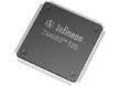
Infineon Technologies 32-bit TRAVEO™ T2G Arm® Cortex® Microcontrollers
Offer cutting-edge performance, safety, and security features for automotive applications.

Infineon Technologies CYT2B7 TRAVEO™ T2G 32-bit Automotive MCUs
Designed for Automotive Body applications such as body control modules, HVAC, and lighting.

Infineon Technologies CYT2BL TRAVEO™ T2G 32-bit Automotive MCUs
Targets automotive systems such as body control units.

Infineon Technologies TRAVEO™ T2G CYT2CL Microcontrollers
Dedicated to automotive systems like cluster entry and body control units.

Infineon Technologies CYT3BB/CYT4BB TRAVEO™ T2G 32-bit Automotive MCUs
Low power consumption MCUs for automotive systems such as high-end body-control units.

Infineon Technologies CYT4BF TRAVEO™ T2G 32-bit Automotive MCUs
Targets automotive systems such as high-end body-control units, zone control, and sound systems.
Related Solutions

Infineon Technologies Automotive Solutions
AEC-Q100 qualified portfolio that consists of high-quality products.