



Infineon Technologies CYT3BB/CYT4BB TRAVEO™ T2G 32-bit Automotive MCUs

Infineon Technologies CYT3BB/CYT4BB TRAVEO™ T2G 32-bit Automotive MCUs target automotive systems such as high-end body-control units. CYT3BB and CYT4BB features one or two Arm® Cortex®-M7 CPUs for primary processing and an Arm Cortex-M0+ CPU for peripheral and security processing. These devices contain embedded peripherals supporting a Controller Area Network with Flexible Data (CAN FD) rate, a Local Interconnect Network (LIN), and Ethernet. TRAVEO™ T2G devices are manufactured on an advanced 40nm process. CYT3BB/4BB incorporates a low-power flash memory and multiple high-performance analog and digital peripherals. The low-power consumption Infineon Technologies CYT3BB and CYT4BB TRAVEO T2G 32-bit Automotive MCUs enable the creation of a secure computing platform.
Features
- CPU subsystem
- 1x or 2x 250MHz (maximum) 32-bit Arm Cortex-M7 CPU, each with
- Single-cycle multiply
- Single/double-precision floating point unit (FPU)
- Memory protection unit (MPU)
- 16KB data cache, 16KB instruction cache
- 16KB instruction and 16KB data tightly coupled memories (TCM)
- 100MHz (maximum) 32-bit Arm Cortex M0+ CPU with
- Single-cycle multiply
- Memory protection unit
- Inter-processor communication in hardware
- 3x DMA controllers
- Peripheral DMA controller #0 (P-DMA0) with 100x channels
- Peripheral DMA controller #1 (P-DMA1) with 58x channels
- Memory DMA controller #0 (M-DMA0) with 8x channels
- 1x or 2x 250MHz (maximum) 32-bit Arm Cortex-M7 CPU, each with
- Integrated memories
- 4160KB of code-flash with an additional 256KB of work-flash
- Read-While-Write (RWW) allows updating the code-flash/work-flash while executing code from it
- Single- and dual-bank modes (specifically for Firmware update Over The Air [FOTA])
- Flash programming through the SWD/JTAG interface
- 768KB of SRAM with selectable retention granularity
- 4160KB of code-flash with an additional 256KB of work-flash
- Cryptography engine
- Supports Enhanced Secure Hardware Extension (eSHE) and Hardware Security Module (HSM)
- Secure boot and authentication
- Using digital signature verification
- Using a fast secure boot
- AES: 128-bit blocks, 128-/192-/256-bit keys
- 3DES: 64-bit blocks, 64-bit key
- Vector unit supporting asymmetric key cryptography such as Rivest-Shamir-Adleman (RSA) and Elliptic Curve (ECC)
- SHA-1/2/3: SHA-512, SHA-256, and SHA-160 with variable length input data
- CRC: supports CCITT CRC16 and IEEE-802.3 CRC32
- True random number generator (TRNG) and pseudo-random number generator (PRNG)
- Galois/Counter Mode (GCM)
- Functional safety for ASIL-B
- Low-power 2.7V to 5.5V operation
- Wakeup support
- Multiple clock sources
- Communication interfaces
- External memory interface
- SDHC interface
- Audio interface
- Timers
- Up to 75x 16-bit and 8x 32-bit timer/counter pulse-width modulator (TCPWM) blocks
- Up to 16x Event Generation (EVTGEN) timers supporting cyclic wake-up from DeepSleep, events trigger a specific device operation (such as execution of an interrupt handler, a SAR ADC conversion, and so on)
- Real-time clock (RTC)
- I/O
- Up to 220x programmable I/Os
- 3x I/O types
- Regulators
- Generates 1.1V nominal core supply from a 2.7V to 5.5V input supply
- 3x types of regulators
- Programmable analog
- 3x SAR A/D converters with up to 75x external channels (72x I/Os + 3x I/Os for motor control)
- Each ADC supports 12-bit resolution and sampling rates of up to 1Msps
- Each ADC also supports up to 6x internal analog inputs such as
- Each ADC supports addressing external multiplexers
- Each ADC has a sequencer supporting autonomous scanning of configured channels
- Synchronized sampling of all ADCs for motor-sense applications
- Smart I/O
- Up to 5x Smart I/O blocks, which can perform Boolean operations on signals going to and from I/Os
- Up to 36x I/Os (GPIO_STD) supported
- Debug interface
- JTAG controller and interface compliant with IEEE-1149.1-2001
- Arm® SWD (serial wire debug) port
- Supports Arm® Embedded Trace Macrocell (ETM) trace
- Compatible with industry-standard tools, GHS/MULTI or IAR EWARM for code development and debugging
- Package options
- 100-TEQFP, 14mm × 14mm × 1.6mm (maximum), 0.5mm lead pitch
- 144-TEQFP, 20mm × 20mm × 1.6mm (maximum), 0.5mm lead pitch
- 176-TEQFP, 24mm × 24mm × 1.7mm (maximum), 0.5mm lead pitch
- 272-BGA, 16mm × 16mm × 1.7mm (maximum), 0.8mm ball pitch
Applications
- Body control modules and body domain control
- Zone control
- Lighting systems
- Cockpit domain control sub-systems
- Sound systems
Block Diagram

Application Notes
- AN218629: Comparison of TRAVEO T1G and TRAVEO T2G
- AN219944: Using the watchdog timer in TRAVEO T2G family MCUs
- AN220152: How to retain RAM data in reset procedure and low-power mode transition in TRAVEO family
- AN220191: How to use Direct Memory Access (DMA) controller in TRAVEO T2G family
- AN220193: GPIO usage setup in TRAVEO T2G family
- AN220224: How to use Timer, Counter, and PWM (TCPWM) in TRAVEO T2G family
- AN220242: Flash accessing procedure for TRAVEO T2G family
- AN220278: CAN FD usage in TRAVEO T2G family
- AN224413: How to Use I2S in TRAVEO T2G family
- AN225346: Using the LIN in TRAVEO T2G family
- AN225401: How to use Serial Communications Block (SCB) in TRAVEO T2G family
- AN226043: How to use sound subsystem in TRAVEO T2G family
- AN229058: Secured Firmware Over-the-Air (FOTA) update in TRAVEO T2G MCU
Additional Resources
Development Tools

Infineon Technologies CYTVII-B-H-4M-176-CPU TRAVEO™ T2G Evaluation Board
A 176-pin evaluation board based on the TRAVEO™ T2G CYT4BB family of devices.
Related MCUs
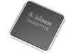
Infineon Technologies 32-bit TRAVEO™ T2G Arm® Cortex® Microcontrollers
Offer cutting-edge performance, safety, and security features for automotive applications.

Infineon Technologies CYT2B7 TRAVEO™ T2G 32-bit Automotive MCUs
Designed for Automotive Body applications such as body control modules, HVAC, and lighting.

Infineon Technologies CYT2B9 TRAVEO™ T2G 32-bit Automotive MCUs
Designed for automotive body electronics with processing power and network connectivity built-in.

Infineon Technologies CYT2BL TRAVEO™ T2G 32-bit Automotive MCUs
Targets automotive systems such as body control units.

Infineon Technologies TRAVEO™ T2G CYT2CL Microcontrollers
Dedicated to automotive systems like cluster entry and body control units.

Infineon Technologies CYT4BF TRAVEO™ T2G 32-bit Automotive MCUs
Targets automotive systems such as high-end body-control units, zone control, and sound systems.
Related Solutions

Infineon Technologies Automotive Solutions
AEC-Q100 qualified portfolio that consists of high-quality products.