Infineon Technologies HybridPACK™ DSC S Modules with SiC MOSFET & NTC
Infineon Technologies HybridPACK™ DSC S Modules with SiC MOSFET and NTC are high-performance power modules designed for demanding automotive applications, particularly in hybrid and electric vehicles (xEVs). This compact half-bridge module integrates silicon carbide (SiC) MOSFETs and an NTC thermistor, enabling superior efficiency and thermal performance. With a blocking voltage of 1200V and a nominal current rating of 190A, the modules support high-speed switching with low conduction and switching losses, thanks to the inherent advantages of SiC technology.This module features a low-inductive design (<8nH) and utilizes double-sided cooling (DSC) for enhanced heat dissipation, allowing operation at junction temperatures up to +175°C. An AlN substrate ensures low thermal resistance, while the integrated NTC sensor provides real-time temperature monitoring for system protection. The FF06MR12A04MA2 is RoHS compliant, UL 94V-0 rated, and validated to Infineon’s automotive standards, making the component a robust and efficient solution for next-generation electric drive systems.
Features
- Electrical
- 1200V maximum drain-source voltage
- 190A implemented drain current
- 380A maximum forward leakage current
- Low (≤8nH) inductive design
- Low drain-source on-resistance
- Low switching losses
- Low total gate charge and reverse transfer capacitance
- Silicon carbide (SiC) semiconductor material
- +175°C temperature under switching conditions
- Mechanical
- 4.25kVDC insulation for 1s
- Compact design
- High power density
- AIN substrate with low thermal resistance
- Integrated NTC temperature sensor
- UL 94-V0 rated module frame
- Qualified according to IFX automotive standard
- RoHS compliant
Applications
- Automotive
- Hybrid electric vehicles [(H)EV]
- Motor drives
Specifications
- MOSFET
- 1200V maximum drain-source voltage
- 190A maximum DC drain current
- 380A maximum pulsed drain current
- Gate-source voltage
- -5/20V maximum static voltage
- -10/23V maximum transient voltage
- 18V on-state gate voltage
- -5V off-state gate voltage
- 14.50mΩ maximum drain-source on-resistance
- 3.25V to 4.55V gate threshold voltage range
- 0.42µC typical total gate charge
- 0.9Ω internal gate resistor
- Typical capacitance
- 10.1nF input
- 0.43nF output
- 0.04nF reverse transfer
- Maximum leakage current
- 100µA drain-source
- 100nA gate-source
- Typical time (inductive load)
- 29ns to 32ns turn-on delay
- 23ns to 25ns rise
- 228ns to 251ns turn-off delay
- 53ns to 62ns fall
- Typical energy loss per pulse
- 7.10mJ to 9.90mJ turn-on range
- 8.30mJ to 9.10mJ turn-off range
- 0.251K/W junction-to-cooling fluid thermal resistance
- -40°C to +175°C temperature range under switching conditions
- Insulation coordination
- 4.25kV isolation test voltage
- AIN internal isolation
- Creepage distance
- 8.5mm terminal-to-heatsink
- 4.3mm terminal-to-terminal
- Clearance
- 8.5mm terminal-to-heatsink
- 3.4mm terminal-to-terminal
- >600 comparative tracking index
- 7.5nH typical stray inductance module
- 0.45mΩ module lead resistance, terminals - chip
- Body Diode (MOSFET)
- 1200V maximum drain-source voltage
- 75A maximum DC body diode forward current
- 380A maximum pulsed body diode current
- 6.88V maximum forward voltage
- 43A to 98A typical peak reverse recovery current
- 0.50µC to 3.40µC recovered charge range
- 0.1mJ to 0.8mJ typical reverse recovery energy
- NTC thermistor
- 5kΩ typical rated resistance
- ±5% Deviation of R100
- 20mW maximum power dissipation
- 3375K to 3433K typical B-value range
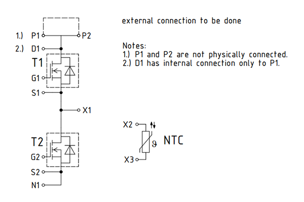
Circuit Diagram

Development Tool
Published: 2025-06-20
| Updated: 2025-07-22


