


NXP Semiconductors LPC80x 32-bit Arm® Cortex®-M0+ MCUs

LPC802 & LPC804 32-bit Arm® Cortex®-M0+ MCUs are low-power, space-efficient, low pin count MCUs based on a 15MHz Arm® Cortex®-M0+ core. NXP LPC802 and LPC804 MCUs support up to 32KB of flash memory and up to 4KB of SRAM.
LPC802 and LPC804 MCUs feature a power-optimized core, a small footprint in popular packages, and level-shifting options thanks to the separate power rails. The peripheral complements of the LPC802 and LPC804 MCUs include a CRC engine, I2C-bus interfaces, up to two USARTs, one SPI interface, and a capacitive touch interface (cap touch). Timer options include a multi-rate timer, a self-wake-up timer, and a general-purpose 32-bit counter/timer. The analog peripherals include a 12-bit ADC, an analog comparator, and on the LPC804, a 10-bit DAC. The LPC802 and LPC804 controllers also feature function-configurable I/O ports through a switch matrix, an input pattern match engine, programmable logic unit (PLU), and up to 30 general-purpose I/O pins.
These 32-bit Arm Cortex-M0+ core MCUs handle 32-bit data more efficiently than 8-bit processors, requiring less code, less memory, and 30% less dynamic power. The low pin count of the LPC802 and LPC804 allows designers to easily share system-critical pins and enable hand-soldering during assembly. Dedicated configurable memory ensures fast initialization at start-up, including pins, clocks, peripherals, and power management.
NXP LPC802 and LPC804 MCUs are supported by NXP's free sample example code bundles, as well as MCUXpresso Integrated Development Environment (IDE) and other popular toolchains, including IAR® and Arm Keil®. LPCXpresso Development Boards offer low-cost evaluation tools and flexible expansion options.
With a power-optimized core and small footprint in popular packages, the LPC80x is a cost-effective Arm Cortex-M0+-based 32-bit MCU ideal for entry level IoT applications.
NXP LPC802 and LPC804 Microcontrollers are offered in a 33-pin HVQFN and 16-pin, 20-pin, and 24-pin TSSOP packages.
Features
- System
- Arm Cortex-M0+ processor (revision r0p1), running at frequencies of up to 15MHz with single-cycle multiplier and fast single-cycle I/O port
- Arm Cortex-M0+ built-in Nested Vectored Interrupt Controller (NVIC)
- System tick timer
- AHB multilayermAtrix
- Serial Wire Debug (SWD) with four break points and two watch points. JTAG boundary scan (BSDL) supported
- Memory
- Up to 32KB on-chip flash programming memory
- Code Read Protection (CRP)
- Up to 4KB SRAM
- Dual I/O power (LPC802M011JDH20, LPC804M111JDH24)
- ROM API support
- Boot loader
- Supports Flash In-Application Programming (IAP)
- Supports In-System Programming (ISP) through USART
- On-chip ROM APIs for integer divide
- Free Running Oscillator (FRO) API
- Digital peripherals
- High-speed GPIO interface connected to the Arm Cortex-M0+ I/O bus with up to 30 General-Purpose I/O (GPIO) pins with configurable pull-up/pull-down resistors, programmable open-drain mode, and input inverter. GPIO direction control supports independent set/clear/toggle of individual bits
- High-current source output driver (20mA) on three pins
- GPIO interrupt generation capability with a boolean pattern-matching feature on eight GPIO inputs. (LPC804)
- Switch matrix for flexible configuration of each I/O pin function
- CRC engine
- Capacitive touch interface (LPC804)
- Programmable logic unit (LPC804)
- Timers
- One 32-bit general-purpose counter/timer, with four match outputs and three capture inputs. Supports PWM mode, and external count
- Multi-rate timer (MRT) for repetitive interrupt generation at up to four programmable, fixed rates
- Self-wake-up timer (WKT) clocked from either free running oscillator (FRO), a low-power, low-frequency internal oscillator, or an external clock input
- Windowed watchdog timer (WWDT)
- Analog peripherals
- One 12-bit ADC with up to 12 input channels with multiple internal and external trigger inputs and with sample rates of up to 480 Ksamples/s. The ADC supports two independent conversion sequences
- Comparator with five input pins and external or internal reference voltage
- One 10-bit DAC (LPC804)
- Serial peripherals
- Two USART interfaces with pin functions assigned through the switch matrix and one fractional baud rate generators
- One SPI controller with pin functions assigned through the switch matrix
- Up to two I2C-bus interfaces.
- Power control
- Reduced power modes: sleep mode, deep-sleep mode, power-down mode, and deep power-down mode
- Wake up from deep-sleep and power-down modes on activity on USART, SPI, and I2C peripherals
- Timer-controlled self-wake-up from sleep, deep sleep, and power-down modes
- Power-on reset (POR) and brownout detection (BOD)
- Additional features
- Unique device serial number for identification
- Single or dual power supplies (1.71V to 3.6V)
- -40°C to +105°C pperating temperature range
Applications
- Sensor gateways
- Simple motor control
- Industrial
- Portables and wearables
- Gaming controllers
- Lighting
- 8-/16-bit applications
- Motor control
- Consumer electronics
- Fire and security applications
- Climate control
Block Diagram

Development Tools
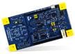
NXP Semiconductors LPCXpresso802 Dev Board (OM40000UL) for LPC802 MCU
Powerful and flexible development tool for the NXP Arm® Cortex®-M0+ based LPC802 Microcontroller.

NXP Semiconductors LPCXpresso804 Dev Board (OM40001UL) for LPC804 MCU
Powerful and flexible development tool for the NXP Arm® Cortex®-M0+ based LPC804 Microcontroller.
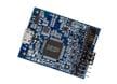
NXP Semiconductors MCU-Link Pro SWD Debug Probe
Feature-rich, low-cost debug tool for Arm® Cortex®-M based microcontrollers.

NXP Semiconductors MCU-Link Debug Probe
Powerful board that can be used with MCUXpresso IDE and is compatible with third-party IDEs.
Related Products
NXP Semiconductors LPC800 Series MCUs
Offer exceptional ease of use, design flexibility, efficiency, and advanced integration.
NXP Semiconductors Semiconductors LPC86x 32-bit Arm® Cortex®-M0+ MCUs
Fully compatible with the Cortex-M architecture and instruction set.
NXP Semiconductors LPC81x & LPC83x 32-bit Arm® Cortex®-M0+ MCUs
32-bit Cortex-M0+ MCUs operating at CPU frequencies of up to 30MHz.
NXP Semiconductors LPC84x 32-bit Arm® Cortex®-M0+ MCUs
Low-power, 30MHz Arm® Cortex®-M0+ core based Microcontroller with advanced power optimization.
NXP Semiconductors LPC82x 32-bit Arm® Cortex®-M0+ MCUs
Designed for higher integration over the LPC81x with a larger memory footprint.