Texas Instruments MSP430F552x/MSP430F551x Mixed-Signal MCUs
Texas Instruments MSP430F552x/MSP430F551x Mixed-Signal Microcontrollers (MCUs) are ultra-low-power MCUs that are configured with an integrated USB and PHY supporting USB 2.0 and four 16-bit timers. These devices include a high-performance 12-bit analog-to-digital converter (ADC), two USCIs, a hardware multiplier, DMA, and an RTC module with alarm capabilities. The MSP430F5528, MSP430F5526, MSP430F5524, and MSP430F5522 microcontrollers include all these peripherals but have 47 I/O pins. The Texas Instruments MSP430F552x/MSP430F551x features a powerful 16-bit RISC CPU, 16-bit registers, and constant generators contributing to maximum code efficiency. The digitally controlled oscillator (DCO) allows the devices to wake up from low-power to active mode in 3.5µs (typical).Features
- 3.6V down to 1.8V low supply voltage range
- Ultra-low power consumption
- Active mode (AM)
- All system clocks are active
- 290µA/MHz at 8MHz, 3.0V, flash program execution (typical)
- 150µA/MHz at 8MHz, 3.0V, RAM program execution (typical)
- All system clocks are active
- Standby Mode (LPM3)
- Real-time clock (RTC) with crystal, watchdog, and supply supervisor operational, full RAM retention, fast wakeup
- 1.9µA at 2.2V, 2.1µA at 3.0V (typical)
- Low-power oscillator (VLO), general-purpose counter, watchdog, and supply supervisor operational, full RAM retention, fast wakeup
- 1.4µA at 3.0V (typical)
- Real-time clock (RTC) with crystal, watchdog, and supply supervisor operational, full RAM retention, fast wakeup
- Off mode (LPM4)
- Full RAM retention, supply supervisor operational, fast wakeup
- 1.1µA at 3.0V (typical)
- Full RAM retention, supply supervisor operational, fast wakeup
- Shutdown mode (LPM4.5)
- 0.18µA at 3.0V (typical)
- Active mode (AM)
- Wake up from standby mode in 3.5µs (typical)
- 16-bit RISC architecture, extended memory, up to 25MHz system clock
- Flexible power-management system
- Fully integrated LDO with programmable regulated core supply voltage
- Supply voltage supervision, monitoring, and brownout
- Unified clock system
- FLL control loop for frequency stabilization
- Low-power, low-frequency internal clock source (VLO)
- Low-frequency trimmed internal reference source (REFO)
- 32kHz watch crystals (XT1)
- High-frequency crystals up to 32MHz (XT2)
- 16-bit timer TA0, Timer_A with five capture/compare registers
- 16-bit timer TA1, Timer_A with three capture/compare registers
- 16-bit timer TA2, Timer_A with three capture/compare registers
- 16-bit timer TB0, Timer_B with seven capture/compare shadow registers
- Two universal serial communication interfaces (USCIs)
- USCI_A0 and USCI_A1 each support
- Enhanced UART supports automatic baud-rate detection
- IrDA encoder and decoder
- Synchronous SPI
- USCI_B0 and USCI_B1 each support
- I2C
- Synchronous SPI
- USCI_A0 and USCI_A1 each support
- Full-speed universal serial bus (USB)
- Integrated USB-PHY
- Integrated 3.3V and 1.8V USB power system
- Integrated USB-PLL
- Eight input and eight output endpoints
- 12-bit analog-to-digital converter (ADC) (MSP430F552x only) with internal reference, sample-and-hold, and auto scan features
- Comparator
- Hardware multiplier supports 32-bit operations
- Serial onboard programming, no external programming voltage needed
- 3-channel internal DMA
- Basic timer with RTC feature
Applications
- Analog and digital sensor systems
- Data loggers
- Connection to USB hosts
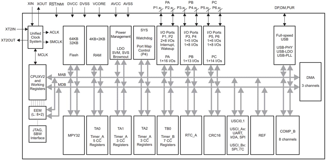
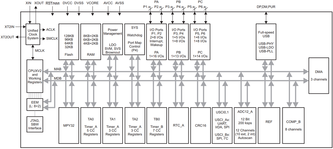
MSP430F551x PN Package Block Diagram

MSP430F551x ZXH ZQE RGC Package Block Diagram

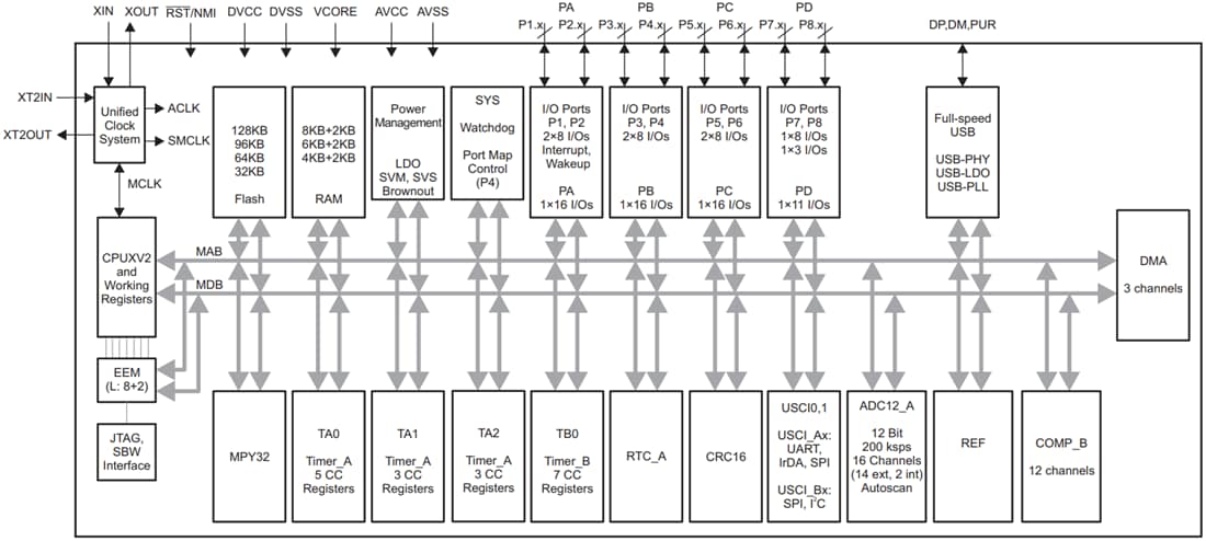
MSP430F552x PN Package Block Diagram

MSP430F552x ZXH ZQE RGC Package Block Diagram

Published: 2020-09-29
| Updated: 2025-04-16


